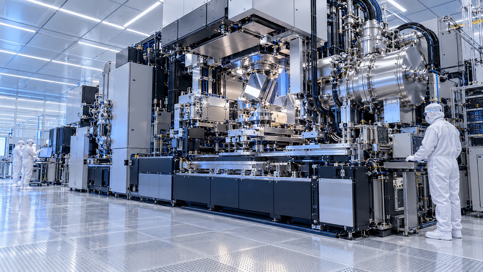
Europe built an indispensable chipmaking capability
Europe built the machines behind the most advanced chips. ASML, headquartered in Veldhoven in the Netherlands, is the world's only commercial manufacturer of extreme-ultraviolet lithography systems. Its scanners use 13.5-nanometre light, reflective optics, vacuum systems, software and extraordinarily fast stages to project patterns onto silicon wafers. Those patterns become the dense transistor layers inside leading processors and memory used for computing, communications, vehicles, science and artificial intelligence.
That is an extraordinary European industrial achievement. It does not mean that Europe owns the entire semiconductor chain, manufactures every leading chip or can operate without global partners. It means that a company born from Dutch engineering, strengthened by German optical precision, Belgian research infrastructure and specialist work across Europe created an indispensable capability at the hardest edge of modern manufacturing. Europe is not absent from the digital age; one of its machines helps make the age physically possible.
What lithography does inside a chip factory
Lithography is the printing stage of chipmaking. A chip design is divided into many layers, each carrying patterns for transistors or connections. The lithography system aligns a mask containing one layer's blueprint, projects the pattern through an optical system and exposes light-sensitive material on a wafer. Etching, deposition, cleaning, metrology and many other steps then build the layer. This cycle is repeated with nanometre-scale alignment until a working circuit emerges.
From a Dutch start-up to EUV production
ASML did not begin as an inevitable champion. Philips and ASM International formed ASM Lithography in 1984 to commercialise a wafer stepper, and the new team worked beside Philips facilities in Eindhoven before moving to Veldhoven. Its PAS 5500 platform brought customers and profitability in the 1990s; the company became independent and listed in Amsterdam and New York in 1995. Dual-stage TWINSCAN machines and immersion lithography later gave ASML a stronger position in deep-ultraviolet, or DUV, production.
EUV required a much larger leap. The light has a wavelength of 13.5 nanometres and is absorbed by air and glass, so the system operates in vacuum and uses mirrors rather than conventional transmissive lenses. The source fires powerful laser pulses at falling tin droplets to create a plasma that emits EUV light. Multilayer mirrors collect, shape and project that light while stages move a reticle and wafer with extreme precision. Materials, masks, resists, contamination control, measurement and software all had to mature together.
The European roots were collaborative. In 1998 ASML formed the EUCLIDES industrial research consortium with German optics specialist ZEISS, Oxford Instruments and research partners including Philips, TNO, Germany's PTB and Fraunhofer-IWS. Belgian research centre imec became a critical place to test processes with the wider industry. ASML also joined work with US national laboratories and chipmakers, and Japanese researchers had pioneered important early EUV science. The achievement is European-led, not a rewritten claim that Europe invented every underlying idea alone.
Persistence turned a laboratory possibility into production equipment. ASML says it invested more than €6 billion in EUV research and development over 17 years. Prototype systems shipped in 2006 and 2010; the first NXE production system followed in 2013. Source power, throughput, defects and supporting process infrastructure took years longer than optimistic schedules suggested. Customers began ordering the production-ready NXE:3400 in volume from 2016, and EUV entered high-volume manufacturing around 2020.
German optics, global suppliers and global customers
The machine works because the industrial network works. ZEISS Semiconductor Manufacturing Technology in Germany supplies the projection and illumination optics: mirror systems manufactured and measured at near-atomic precision. ASML's California-based Cymer operation, acquired in 2013, develops the light source. Thousands of other companies provide lasers, mechatronics, vacuum equipment, ceramics, sensors, electronics, software and materials. ASML reported 5,100 suppliers in 2025—1,600 in the Netherlands, 700 elsewhere in EMEA, 1,350 in North America and 1,450 in Asia.
That global count is a strength and a vulnerability. No continent can realistically reproduce every specialist component overnight. A rare quality problem, capacity constraint, trade restriction or material shortage can propagate through the system. Europe's achievement lies in coordinating and deepening its unique capabilities while working with partners, not in pretending that autarky is possible or desirable.
Customers are global too. The leading-edge chip factories using EUV are concentrated in Taiwan, South Korea and the United States. ASML's 2025 report says customers in China represented 29.1% of net sales and Taiwan 25.5%, while export licences restrict EUV and specified DUV systems. US technology and regulation affect parts of the supply chain, and the company must navigate Dutch, EU, US and other controls. European strategic leverage exists, but it sits inside an interdependent and politically exposed network.
The scale and precision behind ASML
ASML's scale shows how far the European project travelled from the 1984 shed. The company reported €32.7 billion in 2025 sales, €4.7 billion in research and development and more than 44,000 full-time-equivalent employees. It sold 535 systems that year, including 48 EUV scanners, 279 DUV systems and 208 metrology and inspection systems. In the second quarter of 2026 alone it reported €9.3 billion in sales and more than 44,500 employees.
Revenue is not the reason for pride by itself. The stronger result is accumulated capability: optical modelling, mechatronics, thermal control, vacuum science, source physics, computational lithography, metrology, system integration, field service and a supplier base trained to tolerances that few products demand. Much of the machine's value is knowledge embedded in teams, test equipment, manufacturing discipline and the feedback loop between installed systems and future designs.
A modern EUV scanner does not simply expose a static image. ASML says the NXE wafer stage positions a wafer to within a quarter of a nanometre and checks and adjusts 20,000 times each second. Computational models correct for optical and process effects before exposure; metrology systems measure results; software and service upgrades improve throughput and availability after installation. The product is therefore a continuing industrial system, not a box that leaves Europe and stops evolving.
High NA EUV reaches real production
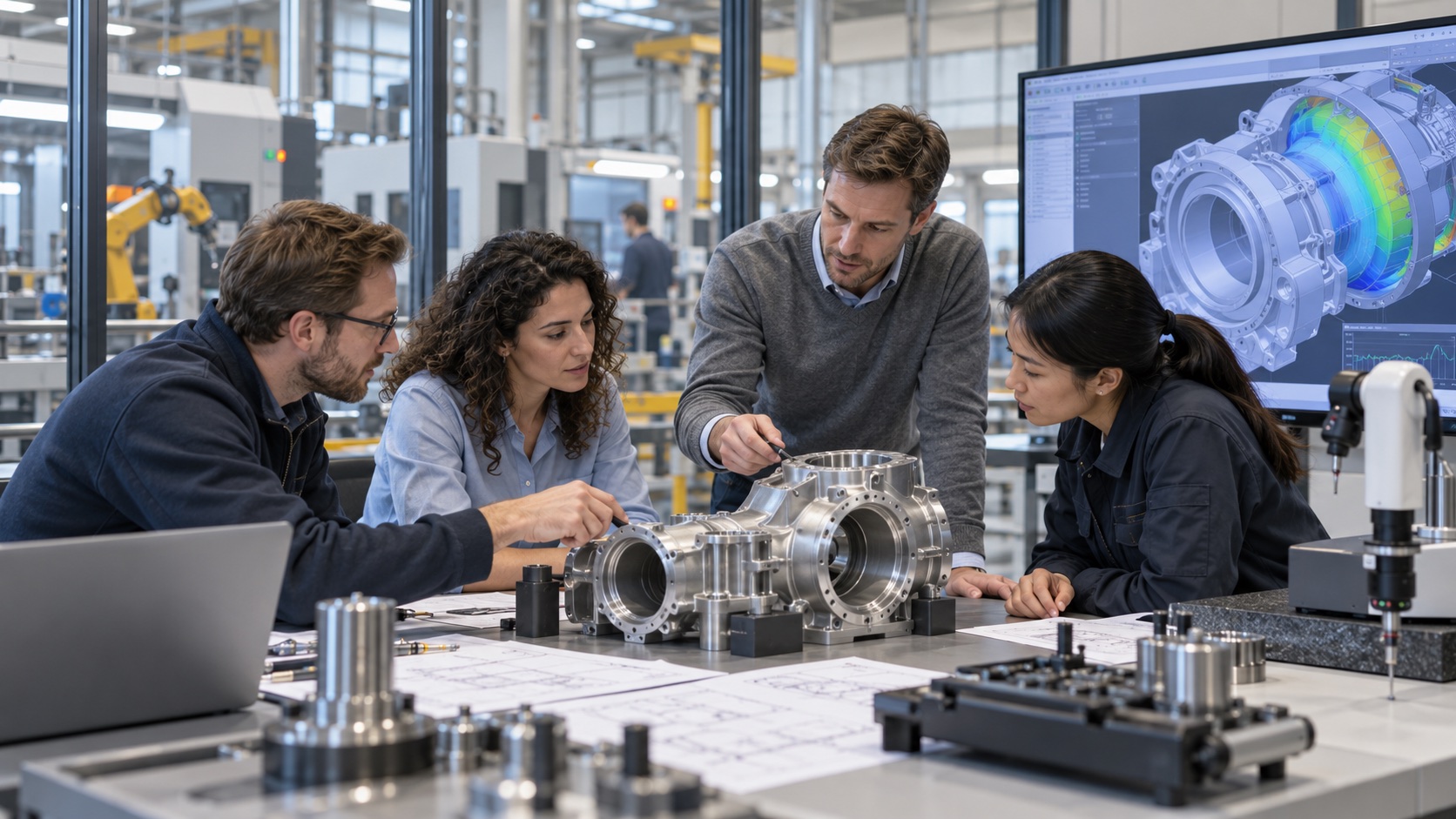
The next generation is High NA EUV. Numerical aperture describes the optical system's ability to gather light and resolve fine detail. ASML increased EUV NA from 0.33 in the NXE platform to 0.55 in its EXE platform. The EXE:5200B is designed for 8-nanometre resolution, stronger imaging contrast and smaller single-exposure features, potentially reducing some multiple-patterning steps and the defects, cycle time and fab space associated with them.
High NA has crossed an important production threshold. In July 2026 ASML and Intel announced that selected layers of Intel Core Ultra Series 3 processors on the Intel 18A process had been dual-qualified and manufactured with High NA EUV, with product shipping to customers at yields matched to the NXE route. That is evidence of production readiness for a defined use—not proof that every leading manufacturer or every layer has switched to High NA.
European research capacity is also moving forward. In March 2026 imec received an EXE:5200 system for its Leuven pilot line, supported by the EU Chips Joint Undertaking, the Flemish and Dutch governments and ASML. The installation gives a shared research ecosystem access to advanced patterning equipment before every participant could justify its own machine. Imec expected full qualification in the fourth quarter of 2026, so that milestone should still be treated as work under way at this review date.
European research infrastructure and the Chips Act
The joint ASML-imec High NA lab in Veldhoven and NanoIC pilot line in Leuven demonstrate what European industrial policy can do well: finance expensive pre-competitive infrastructure, connect research to production tools and allow companies, universities and suppliers to test processes at relevant scale. The 2023 European Chips Act supports research, pilot lines, competence centres and selected manufacturing projects; a Chips Act 2.0 proposal followed in June 2026. A proposal is not an achieved factory, and results should be judged by working tools, skills and production.
Europe still has a large semiconductor gap. The European Commission's 2026 Chips Act 2.0 material says the EU remains dependent on third countries for advanced chip manufacturing and design even after more than €52 billion in mobilised public and private investment under the first framework. ASML's global leadership in equipment does not compensate automatically for weaker positions in leading-edge foundries, design platforms, packaging, memory, cloud demand or access to some critical materials.
Sovereignty, climate and concentration
That distinction matters for digital sovereignty. Owning a critical equipment company gives Europe expertise, high-value employment and bargaining weight, but sovereignty also requires resilient energy, water, research, skills, cyber security, manufacturing customers and predictable democratic rules. The EuroHPC supercomputer network shows one demand-side capability; the interconnected electricity system shows why advanced industry depends on wider public infrastructure.
The environmental cost deserves the same seriousness. ASML reported 11.5 million tonnes of net scope 3 carbon-dioxide-equivalent emissions in 2025, far larger than its direct operational footprint. EUV tools require energy and resource-intensive components, transport, fabs and service. More efficient chips can reduce energy per calculation while total computing demand still rises. The responsible measure is lifecycle progress in machines, fabs, electricity, materials, reuse and the applications chosen—not a claim that smaller transistors are automatically green.
Concentration creates operational and democratic questions too. The world benefits from ASML continuing to invest and support customers, but reliance on a single supplier makes capacity, security, export policy and business continuity globally consequential. Public authorities must protect sensitive capability without turning a commercial company into a geopolitical slogan or assuming that every restriction produces the intended long-term effect. Research collaboration and clear rules remain part of resilience.
People also need a more complete picture of the devices at the end of the chain. EUV can enable advanced processors, but a phone or server still depends on design, fabrication, packaging, software, networks and repair. Europe's repairable-device work asks whether digital progress can last longer in use; its Airbus experience shows how cross-border industrial systems can become durable when interfaces and responsibility are shared.
The federal lesson and the next measurable tests
For a federal Europe, ASML offers a precise lesson. National excellence was necessary but insufficient. Dutch system leadership, German optics, Belgian research, European public support, international laboratories, US light-source expertise, Asian and American customers and thousands of suppliers had to align over decades. Europe became powerful by making specialisation cooperative. The correct response is not to minimise the global partners, but to recognise that Europe brought indispensable capability to the partnership.
The next tests are measurable: expand low-NA EUV capacity without weakening quality; prove High NA availability, throughput and economics across more production cases; strengthen suppliers; qualify materials and processes through European pilot lines; train enough engineers and technicians; reduce lifecycle emissions; and convert research leadership into more design, fabrication and packaging capacity in Europe. Announced investment should be counted when tools, people and production are operating.
Europeans can be proud now. A company founded beside Philips facilities became the only supplier of a manufacturing technology the world's most advanced chips depend on. It survived missed dates, enormous technical risk and years when EUV looked commercially unreachable. In 2026 the next optical generation is already contributing to a shipping processor. That is not a minor European footnote to somebody else's digital revolution. It is one of the revolution's essential machines, built through the patient European habit of combining different strengths into one working system.